南京大学 电子科学与工程学院 江苏省光电信息功能材料重点实验室,南京 210023
结温及载流子温度因作为影响LED发光效率的重要参数而广受关注。文章研究了GaN基蓝光集成传感微小尺寸发光二极管(micro-LED)的光致发光(PL)光谱、载流子温度等随结温的变化规律。通过内置集成传感单元芯片,设计实现了GaN基蓝光micro-LED在0.04~53.4 A/cm2电流密度下结温和PL光谱的实时精确测量,并将正向电压法测量结温的低温端范围拓展至123 K。结果表明,低温下由于载流子泄漏、串联电阻的原因,结温与正向电压的线性斜率发生变化。针对PL光谱使用高能侧斜率法计算得到不同电流密度下的载流子温度,发现载流子温度与结温在所研究的结温和电流密度范围内可以近似用二次方程拟合,并对载流子温度随结温和电流密度变化的规律进行了分析和解释。
微小尺寸发光二极管 电致发光光谱 结温 载流子温度 micro-LED electroluminescence junction temperature carrier temperature
南京大学 电子科学与工程学院 江苏省光电信息功能材料重点实验室, 南京 210023
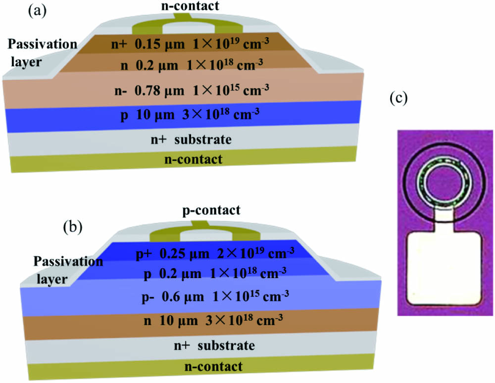
研究了Ag/p-GaN欧姆接触的工艺,得到较为优化的工艺方法并应用于器件制备。分别采用直接剥离Ag、氧等离子体去底胶后剥离Ag和湿法腐蚀Ag三种工艺制备Ag图形,对比了三种工艺样品的粘附性及接触电性,发现直接剥离Ag工艺存在Ag脱落问题,去底胶后剥离Ag工艺无法形成欧姆接触,而腐蚀后退火的样品则可以实现较好的粘附和较佳电性; 通过XPS分析了不同工艺对接触特性影响的机理。进一步,对比优化了Ag蒸发前表面化学处理工艺,结果表明酸性溶液处理或碱性溶液处理可以有效降低欧姆接触电阻率,酸性溶液处理略优。优化后的欧姆接触工艺可应用于可见光及深紫外LED器件制备,器件电学性能如下: 在40A/cm2电流密度下,蓝色发光二极管电压为2.95V,紫外发光二极管电压为6.01V。
欧姆接触 发光二极管 Ag Ag p-GaN p-GaN ohmic contact light emitting diode
本文利用等离子体辅助分子束外延(PA-MBE)系统, 对常规连续外延生长和金属调制外延(MME)生长AlN薄膜进行研究。研究发现: 常规连续外延方法生长模式不易控制, 容易出现过度富Al和富N模式生长, 而且微富Al模式生长还会出现一些凹坑, 表面形貌较粗糙; 然而利用MME方法生长AlN薄膜, 通过精准调控Al源和N源快门打开、关闭时间, 可以获得形貌较好的AlN薄膜。通过调整优化获得的MME方案为: 首先Al源快门打开30 s, 然后Al源和N源快门打开60 s, 最后单独打开N源快门72 s; 单一周期内, Al源快门打开时间与N源快门打开时间比例为0.7。以上述方案为一个周期进行循环生长40个周期, 可获得粗糙度低至0.3 nm(2 μm×2 μm), 几乎无凹坑的AlN薄膜。
金属调制 分子束外延 外延生长 氮化铝 粗糙度 metal modulation molecular beam epitaxy epitaxial growth aluminum nitride roughness
实现电学性能优良的高Al组分AlGaN外延层是制备深紫外光电器件最重要的环节之一。本工作利用分子束外延(MBE)技术, 基于周期热脱附的生长方式, 通过改变Al源供应量调控Al组分, 并用Si进行n型掺杂, 在AlN/蓝宝石衬底上得到了系列高Al组分的Si-AlxGa1-xN外延层(x>0.60)。对外延层相关物理性质进行了表征测试, 结果表明, 外延层Al组分与生长过程中Al束流大小呈现线性关系, 这为制备精确Al组分的AlGaN外延层奠定了基础。AFM结果表明, 高Al组分AlGaN外延层的表面形貌强烈依赖于Ga的供应量, 在生长过程中提高Ga束流可以显著降低外延层的粗糙度。基于范德堡法测量Si-AlGaN外延层电学性能, 证实其载流子特性良好, 其中 Al组分为0.93的样品室温下自由电子浓度、电子迁移率和电阻率分别达到了8.9×1018 cm-3和3.8 cm2·V-1·s-1和0.18 Ω·cm。
高Al组分AlGaN 分子束外延 Si掺杂 载流子特性 周期热脱附 high Al-content AlGaN molecular beam epitaxy Si doping carrier property periodic thermal desorption
1 南京大学 电子科学与工程学院, 南京 210046
2 南京邮电大学 电子与光学工程学院, 南京 210023
3 南京邮电大学 微电子学院, 南京 210023
4 厦门大学, 福建 厦门 361005
基于氮化镓微米LED(Micro-LED)的可见光通信(Visible Light Communication, VLC)技术成为近年来的研究热点。通过深紫外光刻技术制备了小尺寸的氮化镓基蓝/绿光Micro-LED芯片, 深入研究了40~10μm不同尺寸Micro-LED器件的性能, 以及其作为VLC光源的调制带宽能力。研究发现, 随着LED器件尺寸的缩小, 其调制带宽显著增加。通过在电极间加入电磁屏障以及对LED器件侧壁进行钝化修复, 直径为10μm的绿光Micro-LED亮度可达1×10⁸cd/m2, 直径为20μm的蓝光Micro-LED的调制带宽可达372.6MHz。研究结果表明, 基于氮化镓的Micro-LED芯片在调制带宽上仍有较大的提升空间, 经过进一步的研究, 有望推动高速可见光通信的系统应用。
可见光通信(VLC) 调制带宽 氮化镓 visible light communication (VLC) Micro-LED Micro-LED modulation bandwidth GaN

Author Affiliations
Abstract
1 Jiangsu Provincial Key Laboratory of Advanced Photonic and Electronic Materials, School of Electronic Science and Engineering, Nanjing University, Nanjing 210093, China
2 Xiamen University, Xiamen 361005, China
3 e-mail: bliu@nju.edu.cn
4 e-mail: rzhangxmu@xmu.edu.cn
We fabricated p-i-n tunnel junction (TJ) contacts for hole injection on c-plane green micro-light-emitting diodes (micro-LEDs) by a hybrid growth approach using plasma-assisted molecular beam epitaxy (PA-MBE) and metal–organic chemical vapor deposition (MOCVD). The TJ was formed by an MBE-grown ultra-thin unintentionally doped InGaN polarization layer and an layer on the activated layer prepared by MOCVD. This hybrid growth approach allowed for the realization of a steep doping interface and ultrathin depletion width for efficient inter-band tunneling. Compared to standard micro-LEDs, the TJ micro-LEDs showed a reduced device resistance, enhanced electroluminescence intensity, and a reduced efficiency droop. The size-independent J-V characteristics indicate that TJ could serve as an excellent current spreading layer. All these results demonstrated that hybrid TJ contacts contributed to the realization of high-performance micro-LEDs with long emission wavelengths.
Photonics Research
2021, 9(9): 09001683
Author Affiliations
Abstract
1 School of Electronic Science and Engineering, Collaborative Innovation Center of Advanced Microstructures, Nanjing University, Nanjing 210023, China
2 School of Electronic and Information Engineering, Nanjing University of Information Science & Technology Binjiang College, Wuxi 214105, China
Understanding detailed avalanche mechanisms is critical for design optimization of avalanche photodiodes (APDs). In this work, avalanche characteristics and single photon counting performance of 4H-SiC n-i-p and p-i-n APDs are compared. By studying the evolution of breakdown voltage as a function of incident light wavelength, it is confirmed that at the deep ultraviolet (UV) wavelength region the avalanche events in 4H-SiC n-i-p APDs are mainly induced by hole-initiated ionization, while electron-initiated ionization is the main cause of avalanche breakdown in 4H-SiC p-i-n APDs. Meanwhile, at the same dark count rate, the single photon counting efficiency of n-i-p APDs is considerably higher than that of p-i-n APDs. The higher performance of n-i-p APDs can be explained by the larger impact ionization coefficient of holes in 4H-SiC. In addition, this is the first time, to the best of our knowledge, to report single photon detection performance of vertical 4H-SiC n-i-p-n APDs.
4H-SiC avalanche photodiode electron-initiated ionization hole-initiated ionization Chinese Optics Letters
2021, 19(9): 092501
Author Affiliations
Abstract
1 Key Laboratory of Advanced Photonic and Electronic Materials, School of Electronic Science and Engineering, Nanjing University, Nanjing 210023, China
2 Nanjing National Laboratory of Microstructures, Nanjing University, Nanjing 210023, China
3 College of Electronic and Optical Engineering & College of Microelectronics, Nanjing University of Posts and Telecommunications, Nanjing 210023, China
4 Xiamen University, Xiamen 316005, China
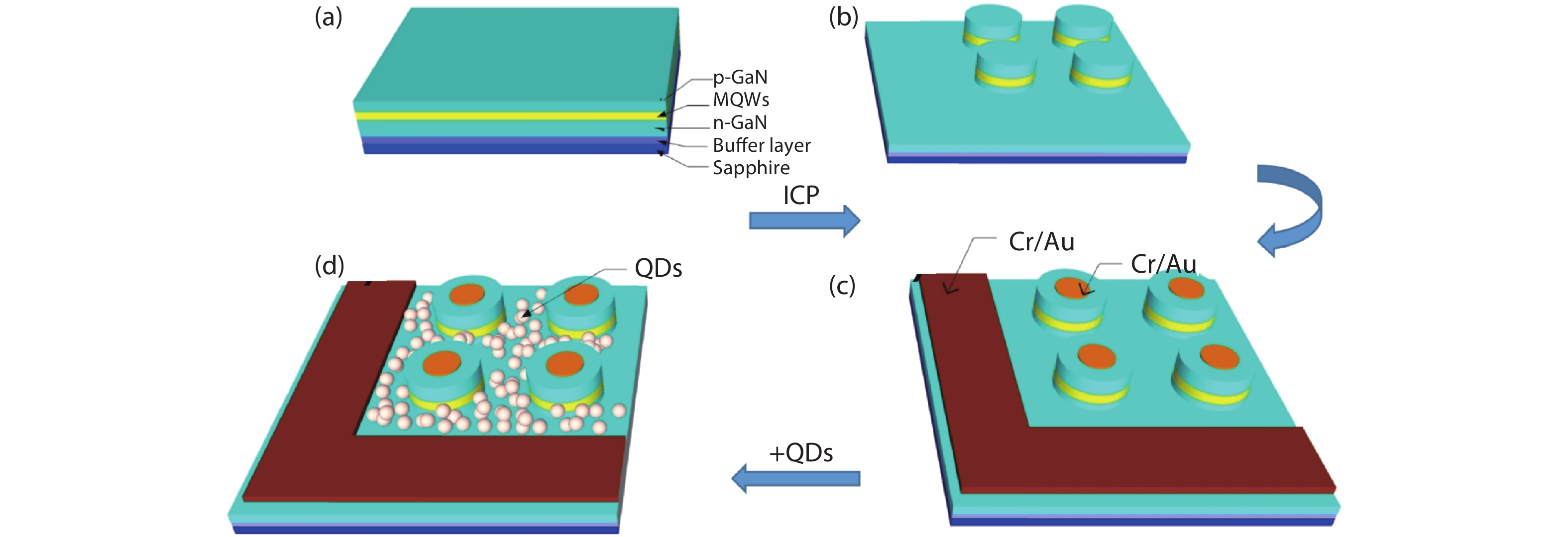
Hybrid white micro-pillar structure light emitting diodes (LEDs) have been manufacture utilizing blue micro-LEDs arrays integrated with 580 nm CIS ((CuInS2-ZnS)/ZnS) core/shell quantum dots. The fabricated hybrid white micro-LEDs have good electrical properties, which are manifested in relatively low turn-on voltage and reverse leakage current. High-quality hybrid white light emission has been demonstrated by the hybrid white micro-LEDs after a systemic optimization, in which the corresponding color coordinates are calculated to be (0.3303, 0.3501) and the calculated color temperature is 5596 K. This result indicates an effective way to achieve high-performance white LEDs and shows great promise in a large range of applications in the future including micro-displays, bioinstrumentation and visible light communication.
Journal of Semiconductors
2020, 41(3): 032301
1 南方科技大学电子与电气工程系,深圳 518055
2 南京大学电子科学与工程学院,南京 210093
现代社会已经进入信息化并向智能化方向发展,显示是实现信息交换和智能化的关键环节。在目前众多显示技术中,MicroLED显示技术被认为是具有颠覆性的次世代显示技术,得到学术界与产业界的广泛关注。MicroLED显示技术是一种新自发光显示技术,具有对比度高、响应快、色域宽、功耗低及寿命长等优点,可以满足高级显示应用的个性化需求。然而目前在MicroLED显示商业化进程中,依然存在一些技术瓶颈尚未解决。应用于MicroLED晶圆的外延技术需考虑衬底选择、波长均匀性及缺陷控制等方面因素;MicroLED器件的效率衰减问题目前依然没有有效的解决途径;此外利用颜色转换媒介实现单片MicroLED全彩显示技术尚未成熟。本文从以上3个问题点出发,分别综述了MicroLED显示目前存在的技术问题及研究现状。
氮化镓 MicroLED显示 外延 MicroLED器件 效率衰减 MicroLED全彩显示 GaN MicroLED display epitaxy MicroLED device efficiency attenuation MicroLED fullcolor display


